EECS 270 Course Projects
Undergraduate Fall 2025 Hardware Grade: A
EECS 270: Introduction to Logic Design transforms basic transistor switching into high-level system design by integrating Boolean algebra, binary arithmetic, and synchronized timing analysis.
Topic 1: Foundations of Hardware Logic
This section explores the bridge between physical signals and logical certainty. By manipulating primitive gates in Verilog, I developed the building blocks of digital systems, from simple data routing to complex arithmetic units.
Project #1: Data Routing & Selection
Project #1: Data Routing & Selection
- Objective: Developing the foundational understanding of hardware abstraction by building a 7-bit data selector to route signals between high-speed input buses and output displays.
- Build: Architected a modular 2-to-1 Multiplexer (MUX) using primitive logic gates (
and,or,not) to manage 7-bit parallel data streams. - Functionality: Integrated the selector with physical FPGA hardware, mapping slide switches to data inputs and pushbuttons to control signals, with real-time feedback on active-low 7-segment displays.
Project #2: Physical Timing & Signal Integrity
Project #2: Physical Timing & Signal Integrity
- Objective: Moving beyond ideal "instant" logic to model the physical reality of electricity and timing constraints within digital circuits.
- Build: Implemented specific gate-level delays (rise/fall times) to analyze signal "drift" and built a Ring Oscillator using a chain of $N$ inverters with feedback.
- Functionality: Conducted timing simulations to observe how gate delays impact system stability, a crucial step for preventing "glitches" in high-frequency robot controllers.
Project #3: Reactive Robot Control (Robbie & Renee)
Project #3: Reactive Robot Control (Robbie & Renee)
- Objective: Designing a functional "brain" for a differential drive robot that transforms multi-sensor inputs into discrete motor commands.
- Build: Developed two versions of the logic: Robbie (binary reactive) and Renee (multi-bit comparison). Implemented an
unsignedCompmodule to prioritize sensor intensity. - Functionality: Created a safety-first priority system where hardware bumpers override environmental sensors to trigger emergency reverse and stop states.
Project #4: Combinational Arithmetic Logic
Project #4: Combinational Arithmetic Logic
- Objective: Building a parameterized 4-bit Arithmetic Logic Unit (ALU) capable of signed mathematical operations.
- Build: Engineered a scalable AddSub module using a chain of Full Adders, utilizing XOR logic to perform subtraction via 2's complement addition.
- Functionality: Implemented real-time hardware error detection (Overflow = $C_{out} \oplus C_{n-1}$) to indicate when results fall outside the representable range $[-8, 7]$.
Topic 2: Sequential Systems & Architecture
By introducing memory, clock-synchronized state, and feedback loops, I moved from static logic to dynamic architectural design, culminating in the creation of a sequential processor that coordinates complex arithmetic operations over multiple cycles.
Project #5: Finite State Machine (FSM) Design
Project #5: Finite State Machine (FSM) Design
- Objective: Implementing the first "memory-aware" system by designing an Up-Down Counter that changes its output based on both current inputs and previous states.
- Build: Developed two architectural variations: a Behavioral FSM using high-level case statements and a Structural FSM using raw Boolean next-state equations.
- Functionality: Simulated a 2-bit saturated counter (often used in CPU branch predictors), tracking "Strong" vs. "Weak" states triggered by synchronized clock edges.
Project #6: Real-Time Traffic Controller (TLC)
Project #6: Real-Time Traffic Controller (TLC)
- Objective: Architecting a complex, multi-flow intersection controller that synchronizes four different traffic directions based on real-time sensor polling.
- Build: Designed a custom Clock Divider to step down the 50MHz FPGA clock to human-perceptible intervals and managed state transitions through a 26-state FSM.
- Functionality: Developed a dual-digit countdown timer and ensured safety-critical transitions (Mandatory Yellow states) across East, West, North, and Side-Road traffic patterns.
Project #7: Sequential Four-Function Processor
Project #7: Sequential Four-Function Processor
- Objective: The capstone project: Architecting an 11-bit sequential arithmetic processor capable of high-performance signed multiplication and division.
- Build: Implemented Booth’s Multiplication Algorithm and a multi-cycle division-by-subtraction routine, coordinated by a central controller that manages a 2x-width shift register (
PM). - Functionality: Built a fully integrated datapath that translates between user-friendly Signed-Magnitude inputs and internal Two's Complement logic, featuring automated overflow protection and an 11-bit binary-to-decimal display driver.
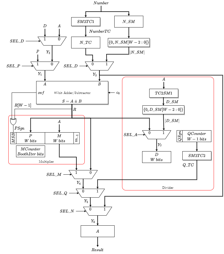 Diagram of the Processor